


Bitte hinterlassen Sie uns eine Nachricht
Privacy statement: Your privacy is very important to Us. Our company promises not to disclose your personal information to any external company with out your explicit permission.
 Guangzhou Quanxu Technology Co Ltd
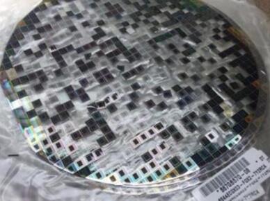
The raw material used for silicon electrical components and silicon photovoltaic cells is silicon ingots. His production includes: ingot growth> ingot cutting and inspection> outer diameter grinding> slicing> round edges> surface grinding> etching> defect removal> polishing> cleaning> inspection> packaging.
1. Ingot growth process
1) Melt
Place the massive high-purity polycrystalline silicon in a quartz crucible and heat it to a melting point above 1420°C to completely melt it.
2) Neck growth
After the temperature of the silicon melt stabilizes, the seed crystal is slowly inserted into it, and then the seed crystal is slowly raised up to reduce its diameter to a certain size, maintain this diameter and extend it by 100 to 200 mm to eliminate the seed crystal The orientation of the grains within is different.
3) Crystal crown growth
After the neck is grown, slowly reduce the lifting speed and temperature to gradually increase the diameter of the neck to the required size (such as 5, 6, 8, 12 inches, etc.).
4) Crystal growth
Constantly adjust the lifting speed and melting temperature to maintain a fixed ingot diameter until the ingot length reaches a predetermined value.
5) The tail grows
When the length of the crystal rod reaches the predetermined value, the lifting speed is gradually increased and the melting temperature is increased, so that the diameter of the crystal rod is gradually reduced, so as to avoid the occurrence of displacement and slippage caused by thermal stress, and finally make the crystal rod and the liquid surface complete Separate. At this point, a complete crystal rod is obtained.
2. Ingot cutting and inspection
Remove the small diameter head and tail of the grown crystal rod, and measure the size to determine the process parameters of the next step.
3. Outer diameter grinding
As the diameter and roundness of the crystal rods have a certain deviation during the growth process, and the outer cylindrical surface is also uneven, it is necessary to trim and grind the outer diameter to make the size and shape errors less than the allowable deviation.
Fourth, slice
Because the hardness of silicon is very high, in this process, a ring-shaped thin slice saw blade with diamond particles inlaid on the edge of its inner diameter is used to cut the crystal rod into slices.

Introduction to the cutting, barrel grinding, etching, slicing, chamfering, grinding and chemical etching of silicon crystal rods.
1. Cut off
The purpose of cutting: cut off the head (seed crystal and shoulder part of silicon single crystal) of the silicon rod along the direction perpendicular to the crystal growth, the tail and the useless part whose outline size is smaller than the specification requirements, and cut the silicon crystal rod into several sections At the same time, cut a sample of the silicon rod to detect its resistivity, oxygen and carbon content, crystal defects and other related quality parameters.
2. Cylindrical barrel grinding
Whether it is a silicon single crystal rod grown by the Czochralski method or the zone melting method, it is generally grown according to the <100> or <111> crystal orientation. Through barrel grinding, the surface can be shaped to meet the basic diameter and diameter tolerance requirements, and the position of the positioning surface and its basic size are determined.
3. Surface corrosion
In order to remove the mechanical damage and contamination of the surface during the grinding process, which is conducive to the subsequent processing, the surface must be chemically corroded.
4. Silicon slice
The single crystal rod is cut into thin wafers with a certain thickness in order to test its main parameters.
5. Wafer chamfering
Its purpose is to eliminate the edges, burrs, chippings, cracks or other defects and various edge pollution caused by cutting on the edge surface of the silicon wafer. After chamfering, the roughness of the edge surface of the silicon wafer can be reduced, and the edge surface of the silicon wafer can be increased. Mechanical strength, reduce surface contamination.
6. Double-sided grinding and surface grinding
In order to remove the surface mechanical stress damage layer and impurity contamination in the previous process, and to make the silicon wafer have a flat surface with a certain geometrical accuracy.
7. Chemical corrosion of silicon wafer
Chemical corrosion can eliminate mechanical stress damage layer and impurity contamination. For large-diameter silicon single wafers, acid etching processes are generally used.
Anticorrosion Pigments, Inkjet Receptive Coating, Matting Agent

November 05, 2024

February 02, 2024

February 02, 2024
Mail an Lieferanten
November 05, 2024
February 02, 2024
February 02, 2024
Über uns
Uns von uns aussagen

Privacy statement: Your privacy is very important to Us. Our company promises not to disclose your personal information to any external company with out your explicit permission.
Fill in more information so that we can get in touch with you faster
Privacy statement: Your privacy is very important to Us. Our company promises not to disclose your personal information to any external company with out your explicit permission.